©±°²³µ¼½¾÷ø
RED ROCK ENERGY
Beam Circuits.

See also:
Beam Circuits Reference Library

Conventions:

  1. When light is applied to an LED the anode sources current and becomes positive.
  2. Most of the LED Sensor circuits are not very sensitive to the power supply voltage, however some are. The ones that specify a VCC of 5 volts have beam tested at that voltage. If a different voltage is used one should verify operation and adjust the resistor components accordingly.
  3. The higher the resistance in the circuitry providing current to the LED the better. I have specified and tested using 22 MOhm resistors. 10 MOhm resistors will work almost as well and can be more easily obtained. I have used 100 MOhm in some of these circuits which greatly improved sensitivity. However be cautious of board and transistor leakage currents.
  4. Almost any low leakage switching transistors can be used. I have mostly used BC337/BC327 transistors. The generic 2N3904/2N3906 work just as well.
  5. I use large 10 mm Lumex green LEDs with a clear case whenever possible, SSL-LX100133XGC. In my testing this LED has been superior to most other LEDs used for light sensing applications. If you want to use a smaller LED select high efficiency types. Select high Lumens per watt types. Don't look for just supper brightness as this has more to do with optical geometry than efficiency.
  6. All the circuits presented can be used in the complementary mode, i.e. swapping all component polarities and swapping NPN for PNP types. An example of this is the beamstepper7 series driving the active low enables of the 74AC240 gates. See below.

a
A
b
B
A
  1. When LED1 is brightly lit it causes Q1 to ground pin 3 of the gate. The voltage dropped by R2 is sufficiently low enough to effect a low on pin 1 & 3.
  2. With less light pin one rises above the threshold and becomes high.
  3. In darkness both inputs are high while pin 3 remains low.
  4. This circuit is sensitive to the power supply voltage. The values given are for 5 volt operation. For other voltages R2 & R3 will need to be adjusted.
B
  1. When LED1 is brightly lit it over powers the lessor lit LED2 causing Q1 to ground pin 3 of the gate. The voltage dropped by R2 is sufficiently low enough to effect a low on pin 1 & 3.
  2. When equally lit pin one rises above the threshold and becomes high while pin 3 remains low.
  3. When LED2 is more brightly lit LED2 absorbs the current from LED1 which turns Q1 off and both inputs are high.
  4. This circuit is sensitive to the power supply voltage. The values given are for 5 volt operation. For other voltages R2 & R3 will need to be adjusted.
g
G
h
H
G
  1. This circuit is a pseudo SCR circuit to form a Schmitt trigger that is normally ON. Unlike an SCR this circuit can be switched off.
  2. Assume LED1 is dark. Current will flow through R3 & R1. This turns on Q2 which cusses current to flow through R2, causing Q4 to turn on. This causes the current flowing through R1 to increase to a higher level latching the circuit ON.
  3. When sufficient light intensity is applied to LED1 it tends to absorb the current flowing through R1. When sufficient current is absorbed Q2 turns OFF, causing Q4 to turn OFF. Current flowing through R1 is reduced to a lower level latching the circuit off as long as sufficient light is applied to LED1.
  4. The light intensity applied to LED1 must go below a lower level to cause Q2 to turn back ON.
H
  1. This circuit is a pseudo SCR circuit to form a Schmitt trigger that is normally OFF. Unlike an SCR this circuit can be switched off.
  2. Assume LED1 is dark. R3 prevents Q4 from turning on. With no current flowing through R1 Q2 will also stay off latching the circuit in the OFF condition.
  3. When sufficient light intensity is applied to LED1 it causes current to flow in the base of Q2 which causes current to flow through R2. This current will be greater than that which can be absorbed by R3 and the excess will turn Q4 ON causing current to flow in R1. The sum of the currents from R1 and LED1 is sufficient to keep the circuit latched in the ON condition.
  4. The light intensity applied to LED1 must go below a lower level to cause Q2 to conduct less current. When the current through R2 is insufficient to overcome the current being absorbed by R3 Q4 will turn OFF.
  5. This circuit is sensitive to the power supply voltage. The values given for a nominal 5 volts with a range of about 2.5 to 7.5 volts. For other voltages R3 will need to be adjusted.
c
C
d
D
C
  1. When LED1 is brightly lit it sources current into the base of Q1, out the emitter, and back around through D2. Q1 being ON grounds R1. Q2 being OFF raises R2 HIGH.
  2. With the illumination on the LEDs about equal both Q1 & Q2 will be OFF raising both R1 & R2 HIGH.
  3. When LED2 is brightly lit it sources current into the base of Q2, out the emitter, and back around through D1. Q2 being ON grounds R2. Q1 being OFF raises R1 HIGH.
  4. At no time can both Q1 and Q2 be on at the same time.
D
  1. When LED1 is brightly lit it sources current into the base of Q1. The current comes from R3. Q1 being ON grounds R1. Q2 being OFF raises R4 HIGH.
  2. With the illumination on the LEDs about equal both Q1 & Q2 will be ON, due to base currents from R2 & R3, pulling both R1 & R2 LOW.
  3. When LED2 is brightly lit it sources current into the base of Q2. The current comes from R2. Q2 being ON grounds R4. Q1 being OFF raises R1 HIGH.
  4. At no time can both Q1 and Q2 be off at the same time.
e
E
f
F
E
  1. This circuit is a pseudo SCR circuit to form a Schmitt trigger that is normally ON. Unlike an SCR this circuit can be switched off.
  2. I will describe the left side operation, the right side operates similarly.
  3. Assume both LEDs are dark. Current will flow through R2 & R5. This turns Q1 ON which cusses current to flow through R1, causing Q3 to turn ON. This causes the current flowing through R2 to increase to a higher level latching the circuit ON. Both sides will be latched ON.
  4. When sufficient light intensity is applied to the LED2 it tends to absorb the current flowing through R2 increasing the drive to Q2. When sufficient current is absorbed Q1 turns OFF, causing Q3 to turn OFF. Current flowing through R2 is reduced to a lower level latching the circuit OFF as long as greater light intensity is applied to LED2.
  5. When sufficient light intensity is applied to LED1 it overcomes the current absorbed by LED2 and can supply current to turn Q1 ON. This in turn causes Q3 to turn ON increasing the current through R2 to a higher level latching the left side ON.
  6. This differential illumination of the LEDs has a dead band where both sides can never be both off.
F
  1. This circuit is a pseudo SCR circuit to form a Schmitt trigger that is normally OFF. Unlike an SCR this circuit can be switched off.
  2. I will describe the left side operation, the right side operates similarly.
  3. Assume both LEDs are dark. R5 absorbs the current through R1 sufficiently to starve the base of Q3 turning Q3 OFF. This turns Q1 OFF which reduces current to flow through R1, causing Q3 to turn OFF latching the circuit OFF. Both sides will be latched OFF.
  4. When sufficient light intensity is applied to the LED1 it tends to source current to the base of Q1 turning Q1 ON. The current flowing in R1 is sufficient to overcome the current absorbed by R5 causing Q3 to turn ON which causes current to flow through R2 combined with that from LED1 bringing the base drive of Q1 to a higher level latching the circuit ON as long as sufficient light is applied to LED1.
  5. When sufficient light intensity is applied to LED2 it absorbs the current from LED1 and R1 starving Q1 of base drive switching Q1 OFF which in turn causes Q3 to turn OFF latching the circuit OFF.
  6. This differential illumination of the LEDs has a dead band where both sides can never be both on.
  7. This circuit is sensitive to the power supply voltage. The values given for a nominal 5 volts with a range of about 2.5 to 7.5 volts. For other voltages R5 & R6 will need to be adjusted.
k
K
l
l
K
  1. This circuit has greatly improved sensitivity in low light conditions.
  2. This circuit is a pseudo SCR circuit to form a Schmitt trigger that is normally ON. Unlike an SCR this circuit can be switched off.
  3. Assume LED1 is dark. Q6 will not have any base current nor collector current. Current will flow through R3 & R1. This turns on Q2 which cusses current to flow through R2, causing Q4 to turn on. This causes the current flowing through R1 to increase to a higher level latching the circuit ON.
  4. When sufficient light intensity is applied to LED1 it sources current into the base of Q6 which absorbs the current flowing through R1. When sufficient current is absorbed Q2 turns OFF, causing Q4 to turn OFF. Current flowing through R1 is reduced to a lower level latching the circuit off as long as sufficient light is applied to LED1.
  5. The light intensity applied to LED1 must go below a lower level to cause Q2 to turn back ON.
L
  1. This circuit has greatly improved sensitivity in low light conditions.
  2. This circuit is a pseudo SCR circuit to form a Schmitt trigger that is normally ON. Unlike an SCR this circuit can be switched off.
  3. I will describe the left side operation, the right side operates similarly.
  4. Assume both LEDs are dark therefore Q5 & Q6 are OFF. Current will flow through R2 & R5. This turns Q1 ON which cusses current to flow through R1, causing Q3 to turn ON. This causes the current flowing through R2 to increase to a higher level latching the circuit ON. Both sides will be latched ON.
  5. When sufficient light intensity is applied to the LED1 it sources current into the base of Q5, out the emitter, and back through D2. Q3 absorbs the current flowing through R2 decreasing the drive to Q1. When sufficient current is absorbed Q1 turns OFF, causing Q3 to turn OFF. Current flowing through R2 is reduced to a lower level latching the circuit OFF as long as greater light intensity is applied to LED1.
  6. When sufficient light intensity is applied to LED2 it overcomes the current sourced by LED1 which starves Q5 turning Q5 OFF and allows R2 to supply current to turn Q1 ON. This in turn causes Q3 to turn ON increasing the current through R2 to a higher level latching the left side ON.
  7. This differential illumination of the LEDs has a dead band where both sides can never be both off.
i
I
j
J
I
  1. R1 & R2form a voltage divider at 1/2 of the supply.
  2. When both LEDs are dark or illuminated equally current can neither flow into Q1 nor Q2. Especially since the two bases are connected together resulting in Q3 & Q4 being both OFF.
  3. With Greater illumination on LED1 current is sourced into Q1 resulting in Q3 also being ON. Q4 is also OFF.
  4. With Greater illumination on LED2 current is sourced into Q2 resulting in Q4 also being ON. Q3 is also OFF.
  5. At no time can Q3 or Q4 be on at the same time.
J
  1. R1 & R2form a voltage divider at 1/2 of the supply.
  2. The top half operates essentially independent of the lower half.
  3. When LED1 is dark current from R1 flows into the base of Q1 and through it's emitter into the lower half circuitry. This cusses Q1 to be turned ON resulting in Q3 being ON.
  4. When LED1 is illuminated sufficiently to absorb the current flowing through R1 Q1 is starved of base current and is OFF causing Q3 to also be OFF.
  5. When LED2 is dark current from R1 flows into the base of Q2 and through it's emitter into the lower half circuitry. This cusses Q2 to be turned ON resulting in Q4 being ON.
  6. When LED2 is illuminated sufficiently to absorb the current flowing through R2 Q2 is starved of base current and is OFF causing Q4 to also be OFF.
  7. This is an interesting circuit in that it has 4 distinct states as opposed to most of the other LED sensor circuits having 2 or 3 distinct states.

3
beamstepper3
Bipolar Stepper Motor Driver based on a CMOS 40106 Hex Schmitt Trigger Inverter.

Wilf's description.

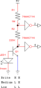
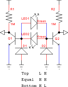
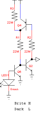
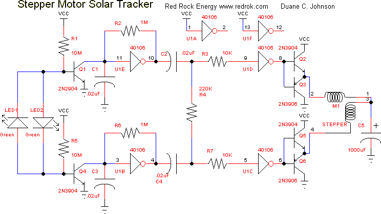
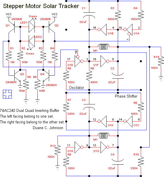
The stepper controller operation is as follows (I think):

The LED photo detectors work together with Q1 and Q4 to enable either of the two independent oscillators. When the LEDs are aligned with the sun, both LED sensors would be shaded by a "shadow mask", both Q1 and Q4 are on and both oscillators are disabled.
( Actually you don't need the shadow mask. Both transistors will be ON whether there is no light on the LEDs or both LEDs have the same illumination. Either way they will have zero volts across the LED pair. Redrok. )

When one or the other LED is illuminated, the transistor is turned off and the oscillator is enabled and generates a square wave.

The LED photo detector uses it's photovoltaic output voltage to drive the transistor base negative and the transistor turns off.

Assume that LED1 is lit. LED1 anode voltage remains at +0.6V (clamped by the Q4 base-emitter) but the LED generates a negative voltage at the cathode of -1V which drives the Q1 base negative and turns off Q1 collector current. That releases the U1E input and the oscillator starts.

This is where the circuit gets funky: The outputs of the oscillators are connected to a "floating" RC network i.e. a network that has no DC connection to the supply rails. External leakage currents can cause the DC level in such a network to drift. Despite the lack of a DC reference, the average DC level of this network must hover near VCC/2 for it to operate.

Measuring waveforms in this floating network with a scope probe can cause problems as the probe has a 1M or 10M (x10 setting) impedance to GND.

I would recommend adding a high resistance voltage divider between VCC and GND with the midpoint connected to the network to stabilize the DC level of the network to VCC/2 or better yet just below the lower trigger threshold (approximately VCC/3)

Keeping in mind, the necessary floating DC level of the network, the AC coupled waveforms, superimposed on the DC level will cross the thresholds of the Schmitt triggers as required.

The U1E oscillator output is capacitively coupled via C2 through R3 to the input of U1D. The signal will be clamped by the input protection network to VCC+.6V. The output of U1D will follow the input without delay. The coupled signal from C2 also drives an integrating RC network formed by R4 and C4. This causes a delayed signal of VCC/2 superimposed on the DC to appear at the input of U1C. Since the normal positive switching threshold of the Schmitt trigger is 3V. See the spec:
40106
This VCC/2 signal by itself is not high enough to trigger the input of U1C. However with the added DC level, the signal crosses the threshold of U1C causing a delayed negative output pulse at the output of U1C.

When the U1E oscillator output goes negative, the signal is coupled to the U1D output without delay and through R4 and delayed by C4 the signal appears at the output of U1C.

The result is a quadrature phase relationship between the signals on U1D and U1C with the U1C output delayed.

Now look at the output circuit (quite weird in the best BEAM tradition). When the oscillators are disabled the outputs of U1C and U1D are both at VCC and the capacitor C1 is charged through Q2 and Q5 via the stepper coils to VCC.

Each output is buffered with a voltage follower half bridge power stage.

When the outputs of U1C and U1D are pulsing, the average value of the voltage on C1 is VCC/2 as the cap is alternately partially charged and partially discharged through the stepper coils. The result is a bipolar current waveform through each coil in quadrature that steps the motor in one direction.

The action is the same for the case of LED2 illuminated except that the delayed quadrature signal will be on U1D and the motor steps in the reverse direction.


4a
beamstepper4a
Fully fleshed out Solar tracker based on the 40106.

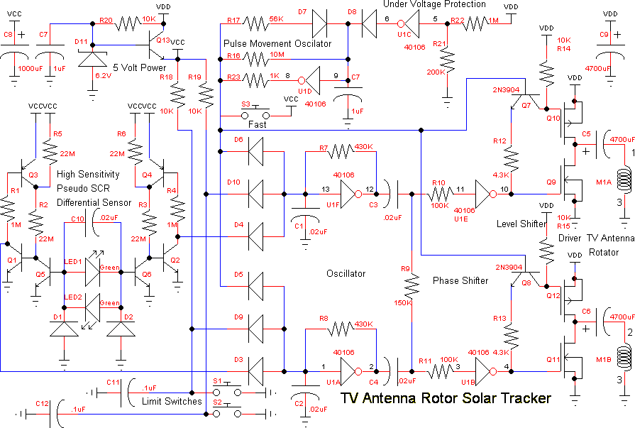
This is the complete circuit. It is designed to drive TV antenna rotators which operate in a similar manor to a stepper motor. In this case the motor is a capacitor run motor. The circuit provides the 90 degree quadrature drive for reversing motion. Vdd should be be about 30 to 40 volts.

The sensor is the high sensitivity High sensitivity pseudo SCR sensor. Steering diodes are added to isolate the several functions. Note the capacitor C10 to prevent or dampen mechanical oscillations.

Limit switches are added to limit extended movement.

A pulse oscillator is added to slow down mechanical movement. The movement is accomplished by delivering about 4 phase shifted cycles to the motor every 10 seconds or so. A manual Fast switch allows quick movements.

The level shifter is used to drive the power MOSFETs which deliver about 3 amps to the motor. An under voltage protection circuit prevents damage to the upper MOSFETs if Vdd gets below about 15 volts.

5 volts Vcc is regulated from Vdd.


7e2
beamstepper7e2
Bipolar Stepper Motor Driver based on a Dual Quad Buffer

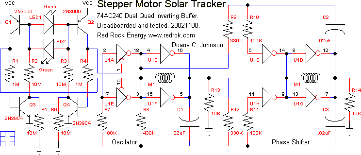
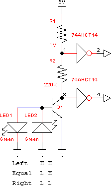
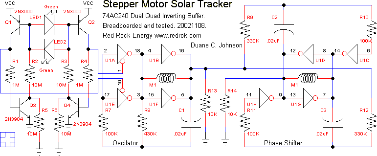
Wilf and I have been developing another solar tracker that is based on a 74AC240 Dual Quad Tristate Buffer. There have been a number of variations. These are the results.

The 74AC240 stepper driver works by enabling each half of the buffer. Only one half can be enabled at a time.

Let's assume that the top half of the driver is enabled. U1A & U1B along with R8, C1, & the input protection resistor R7 form a square wave oscillator. The outputs of U1A & U1B directly drive one coil of a bipolar stepper motor.

U1C & U1D along with R9, C2, & the input protection resistor R10 form a 90 degree phase shift. The outputs of U1C & U1D directly drive the other coil of the bipolar stepper motor. The motor turns in one direction.

If the second bottom half of the driver is enabled the oscillator using U1E & U1F work as before. U1H & U1G along with R12, C3, & the input protection resistor R11 form a 90 degree phase shift. Except it's connected the other way around from before so it's actually 270 degrees. The outputs of U1H & U1G directly drive the other coil of the bipolar stepper motor. The motor turns in the other direction. Neat, Huh!

An earlier version of the circuit didn't work well because the the sensors presented an analog enable signal. This was sometimes at the threshold voltage which caused the buffer to have high idle current and sometimes cross coupling which was a bad thing. %^(

What was needed was a sensor that had a Schmitt trigger input. This could be done using a Schmitt trigger gate which works well. I suggest a 40106 or 74AHCT14. However, this needs a second IC.

A better solution is to make the sensor have Schmitt action. The first version was:
Normaly OFF pseudo SCR sensor
The problem was that the pseudo SCR circuit worked over a limited voltage range.

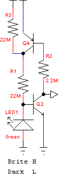
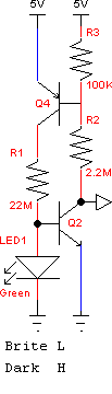
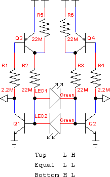
Normaly ON pseudo SCR sensor
works better. Q1 & Q3 and Q2 & Q4 each form a bistable latch similar in operation to an SCR.

Let's start with the left side without the LEDs. Initially no current flows. The series resistors R5 & R2 cause a small bias current to flow in the base of Q1, which reflects current through R1 causing Q3 to conduct. Since Q3 shorts out R5 the current through R2 doubles. The output at the collector of Q1 snaps high disabling the connected buffers.

(Note, R5 & R6 aren't actually required. It turns out that leakage currents in the transistors is enough to get started. I tried many transistors and never found one that didn't work as expected. Prudent circuit design demands that R5 & R6 be included because one might find a transistor that is so perfect it won't work. Bummer. )

The now connected and lit LED1 has the ability to absorb the current through R2 starving Q1 which switches off resulting in the output snapping low. Q3 also switches off reducing the bias current in R2 to 1/2. This condition persists until the LED goes dark.

You might ask where the current for the other side of the LED comes from. It is from base of Q2 on the right side. Actually, when the left side is turned off the right side is turned on doubly as the current from both R2 and R3 go through the base.

The right side works the same way. Since the LEDs are connected anti parallel only one latch can be off at a time. This is safe for the buffers.

When both of the quad buffers are supposed to be off it is essential that all inputs not be near the threshold to have the lowest idle current. R13 & R14 ensure that all inputs be near ground. All inputs are connected to R13 or R14 either directly, through input resistors, or through the stepper motor windings. R13 & R14 can also be connected to VCC. They don't even need to be to the same voltage, although it operates quicker if they are the same voltage.

I have tested this circuit with about 25 different 74AC240s. They all worked as expected.

I ran the circuit from about 2.4V to 8.5V. OK, one shouldn't go past 7V to be within the specs of the 74AC240. I even have found some 74AC240s that worked to 14V, but I wouldn't recommend this.

The sensor section was tested to 40V. It still worked well, the sensitivity is less because the bias currents are proportional to voltage which requires brighter illumination to work properly.

The step patterns are not perfectly symmetrical because this is essentially an analog circuit. Some resistor adjustment may be needed.

To change the speed of the motor adjust the capacitor values. Note, all three need to be the same value.

I have chosen the time constants of R9-C2 & R12-C3 to be about 3/4ths of R8-C1. Try to keep these ratios. ( BTW, I'm not sure this is the exact ratio but it seams about right. )

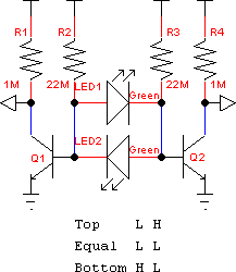
The 10M resistors in the sensor are the largest commonly available resistors in 1/8W size. I tried 22M in 1/4W and that worked well with added sensitivity. I suppose if you could find 100M they would work even better. However be careful of leakage currents on the board and transistors.

I have a variation which is even more sensitive to low light levels. See:
High sensitivity pseudo SCR sensor


7e1
beamstepper7e1
Bipolar Stepper Motor Driver based on a Dual Quad Buffer
Optimized for circuit layout

This variation uses the same number of parts but has a better layout.

The description of operation is the same as the above circuit except the phase shifter is reversed and connected to a single point on the oscillator.

This might have an application using a 74AC125 quad single mux where another oscillator may be present.


7e3
beamstepper7e3
Bipolar Stepper Motor Driver based on a Dual Quad Buffer

My first attempt, note the neat circuit symmetry.


ledtri
LED PSH H-Bridge
I added the an LED sensor to Wilf's Tri-Bridge.

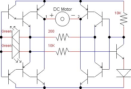
I needed to drive the right side of the bridge with an inverted signal. This signal is not available on the left side. I needed to add an inverter. The inverter has a 10K collector load resistor. This pulls up the right side when the left side is low. When the left side goes hi the inverter transistor is turned on pulling the right side low.

The PSH H-Bridge circuit has a curious quirk. It doesn't work well when on input is pulled to a supply rail. The problem is that the driver transistor can only saturate so much. This starves the output transistor of base current. The simple solution is to have either an input resistor or limit the voltage with a diode as I did here.

Neat bridge.


ledtri2
LED PSH H-Bridge 2
This works much better.

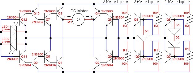
In the last version of this LED bridge the operation was limited to about 3.6V or higher. In this version I attempted to make it work at a lower voltage with greatly improved sensitivity.

LED1 & LED2 along with Q11 & Q12 form a sensitive light to current amplifier. Only one of these transistors can be ON at the same time. Let's assume LED1 is lit. Q12 supplies amplified LED current to Q10 then Q7 then to output transistor Q3. In addition Q7 passes triply amplified LED current out it's emitter and into the emitter of Q6 which transfers that current out Q6's collector and into the base of output transistor Q2. R1 & R2 form a voltage divider at half of the supply. This assists in turning on Q6.

This circuit is essentially analog in nature. The current driven into the motor is proportional to the difference of the current supplied by the LED pair. So when equally lit, or dark, the current goes to zero.

I found that the first version works well from 2.9V on up. To improve this I added D1 which extends operation down to about 2.5V. Both of these versions have low idle currents primarily from R1 & R2.

By adding a second diode, D2, operation works down to about 1.9V. However, the idle current is higher. About 1mA at 1.9V to about 10mA at 5V.

The circuit is quite sensitive to ordinary room light in my lab, lit with fluorescent lights. Just orienting the plug board on the table changes the motor from full forward to reverse. A slight wave of the hand has a dramatic effect. Very sensitive.